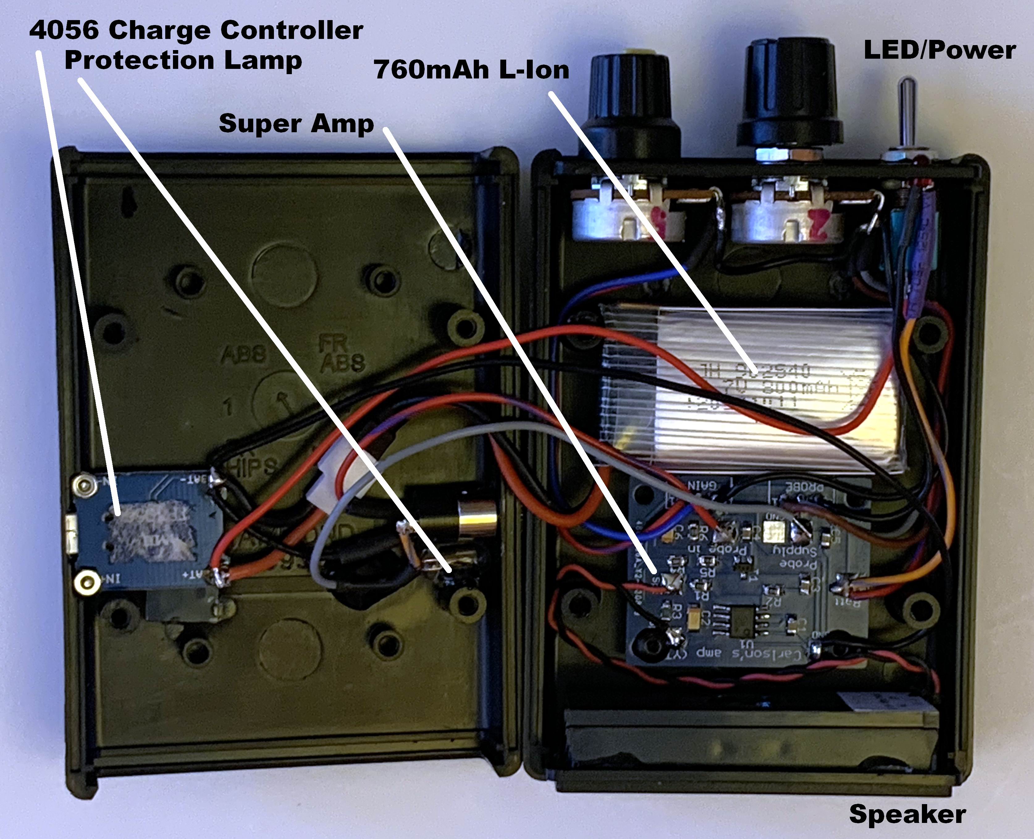
Figure 1
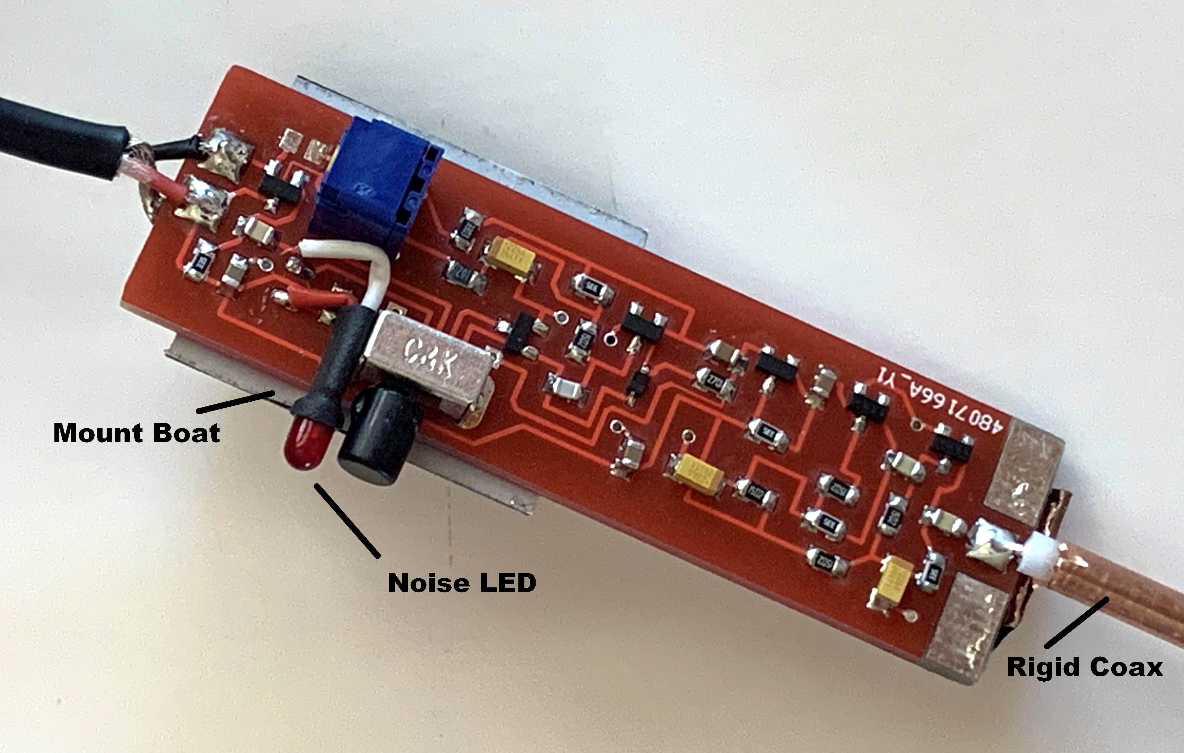
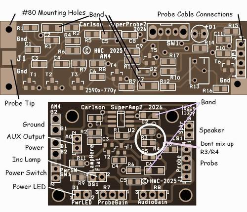 Figure 2
 Figure 3
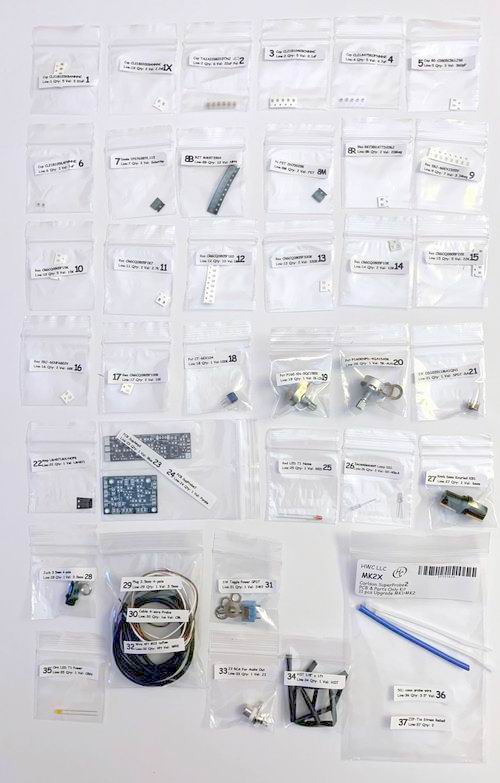 Figure 4
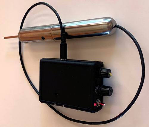 Figure 5
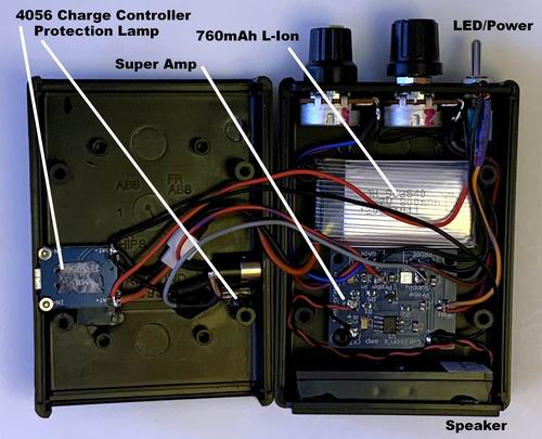 Figure 6
|
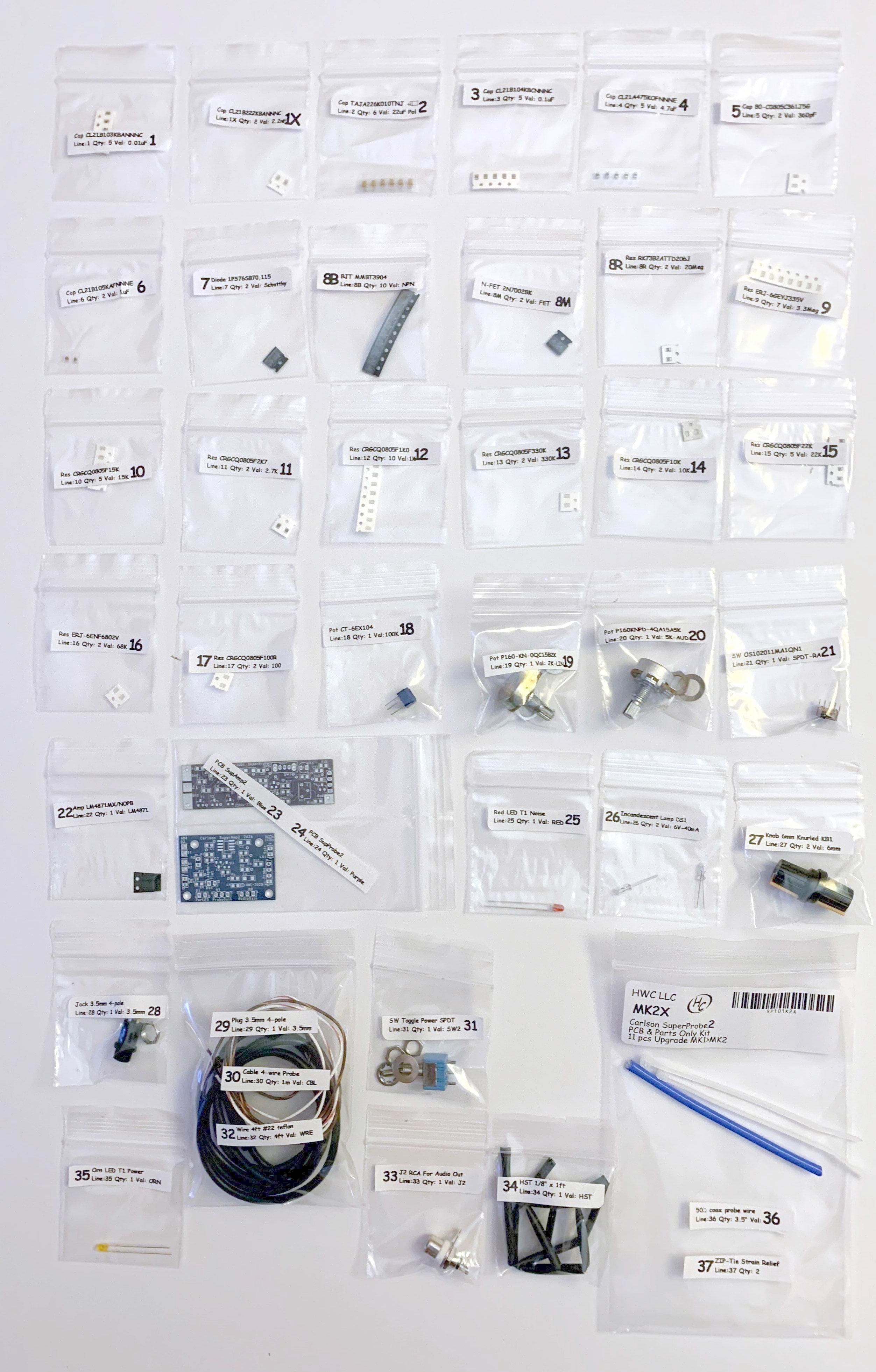
Improved MK2 Kit with 37 Unique Parts
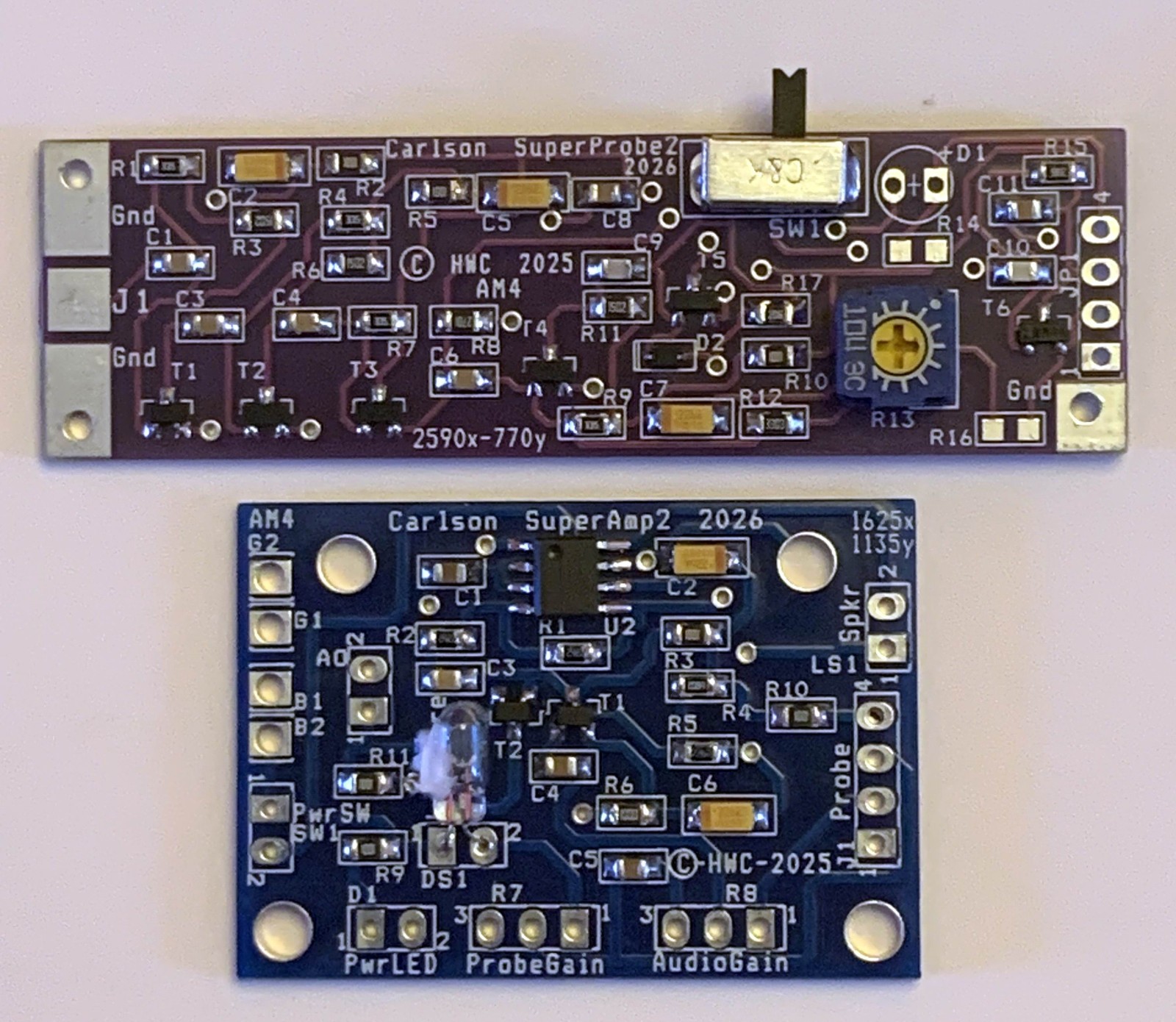
This is our MK2 PCB Kit fully assembled & tested.
As seen on YouTube and commented on many other sites, Paul Carlson designed a very useful non-contact
very high gain electronic probe for investigating just about any kind of electrical signal from audio to RF.
The design is well proven and open-sourced. There are also several open-source PCB designs for the probe and
amplifier, but most of them are SMD designs. This is likely the primary barrier to building a one-off
implementation of this design.
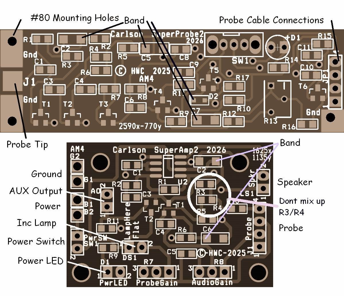
These 2 PCBs are well designed and reliable, and used in many DIY probes.
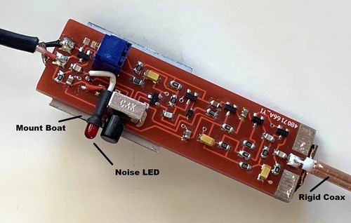
New and improved probe PCB with thru-hole wiring connections, improved SMD component orientation and
easier assembly. The POP noise LED driver is improved. The amplifier POT protection lamp is PCB mounted, and the
amplifier has a new buffered audio output driver.
Anyone interested in building the probe should first review:
Mr Carlson's YouTube video @ https://www.youtube.com/watch?v=uVkJqqZroN0
Yannick99 @ https://www.instructables.com/Carlsons-Super-Probe/
Web search for many other reviews and assembly hints.
Here is a great UT video of Carlson using the SuperProbe to locate a noisy component inside a complex transceiver.
He makes it seem so easy, and with the SuperProbe it is!
https://www.youtube.com/watch?v=uiK1BD7HILo
The Kit:
This MK2ASM kit includes the main PCBs fully assembled and tested and nearly everything else but cases for the probe and amplifier, a battery and a speaker.
See the parts list for what is included.
The kit includes the PCBs as well as the 2 pots (with knobs) used in the amplifier,
protective lamp, #22Ga teflon hookup wire, heat shrink tube, probe-tip, power switch & LED, probe-to-amp wire, 3.5mm 4-wire plug and jack.
It DOES NOT include cases, packaging, screws, batteries, speaker, or anything else that might be needed to
construct a complete SuperProbe.
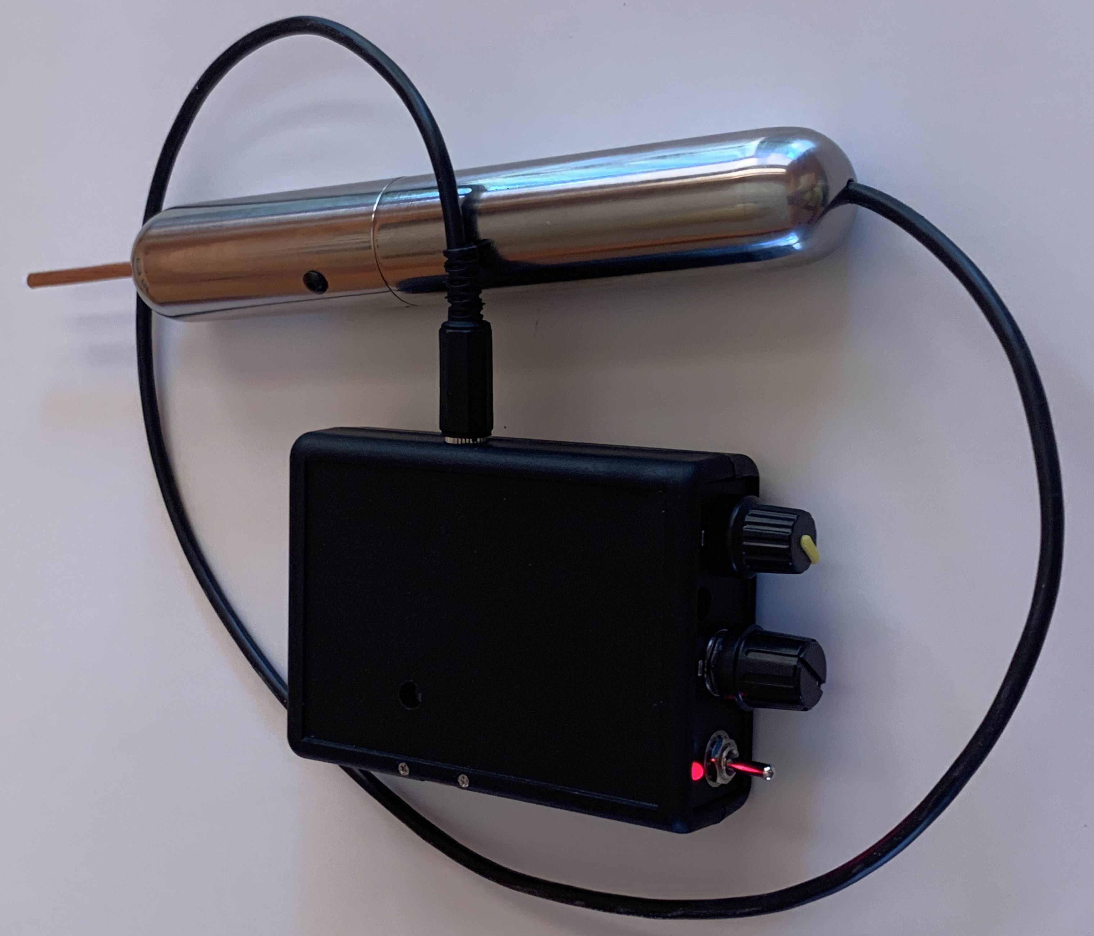
The black ABS case shown in the pictures is made by Hammond, part #1593LBK 3.6" x 2.6" x1.1". Nothing smaller is really suitable.
The Assembly:
Follow the included instructions in detail. Schematic details are included and are identical to the original design.
Some of the listing photos show a particular implementation in a very compact package. Such compactness is not necessary, but demonstrates what can be achieved.
We recommend cleaning flux after assembly. This is a very sensitive device and leakage is undesirable. If water soluble flux/water is used, be careful
cleaning the switch & POT.
|
|